ดาวน์โหลดงานนำเสนอ
2
322 361 Computer Systems Architecture บทที่ 4 Mem ory Spy 002 Top Secret

3
2 หัวข้อเรื่อง หลักการทำงาน ของ RAM Modules of RAMs Memory Cycle Error Checking Technology of RAMs

4
3 วัตถุประสงค์การ เรียนรู้ อธิบายโครงสร้างหลักๆ ของ หน่วยความจำได้อย่างละเอียด ยกตัวอย่างรูปแบบต่างๆ ของ Semi-Conductors อธิบายโครงสร้างการกำหนด ตำแหน่งได้ อธิบายความสำคัญและ โครงสร้างของหน่วยความจำ แคชได้ ยกตัวอย่างรูปแบบต่างๆ ของ Semi-Conductors

5
4 RAM Random Access Memory Read/Write Access Memory หน่วยความจำหลักที่ใช้ใน ปัจจุบันทำงานแบบ Random Access Memory สามารถอ่าน - เขียน โดยตรงด้วย wired-in addressing logic Table 4.2 Volatile Memory

6
5

7
6 RAM ใช้ Flip-Flop Logic Gate เป็นตัวกำหนดค่า ข้อมูล (Binary Value) สามารถเก็บข้อมูลได้ตราบ เท่าที่มีกระแสไฟฟ้าส่งมา หล่อเลี้ยง สามารถเข้าถึง ข้อมูลได้อย่างรวดเร็ว Static RAM (SRAM)
 สามารถเก็บข้อมูลได้ตราบ เท่าที่มีกระแสไฟฟ้าส่งมา หล่อเลี้ยง สามารถเข้าถึง ข้อมูลได้อย่างรวดเร็ว Static RAM (SRAM)")
8
6 transistors CMOS SRAM cell.

9
8 RAM เป็น cell ที่จัดเก็บข้อมูล โดยการส่งกระแสไฟฟ้ามา จากตัว capacitors ซึ่ง ต้องจัดส่งมาเป็นระยะๆ เพื่อรักษาข้อมูลที่จัดเก็บไว้ ด้วย (Periodic) มีวงจรที่ อัดแน่นได้มากกว่า จึงมี ราคาที่ถูกกว่า Dynamic RAM (DRAM)
 มีวงจรที่ อัดแน่นได้มากกว่า จึงมี ราคาที่ถูกกว่า Dynamic RAM (DRAM)")
11
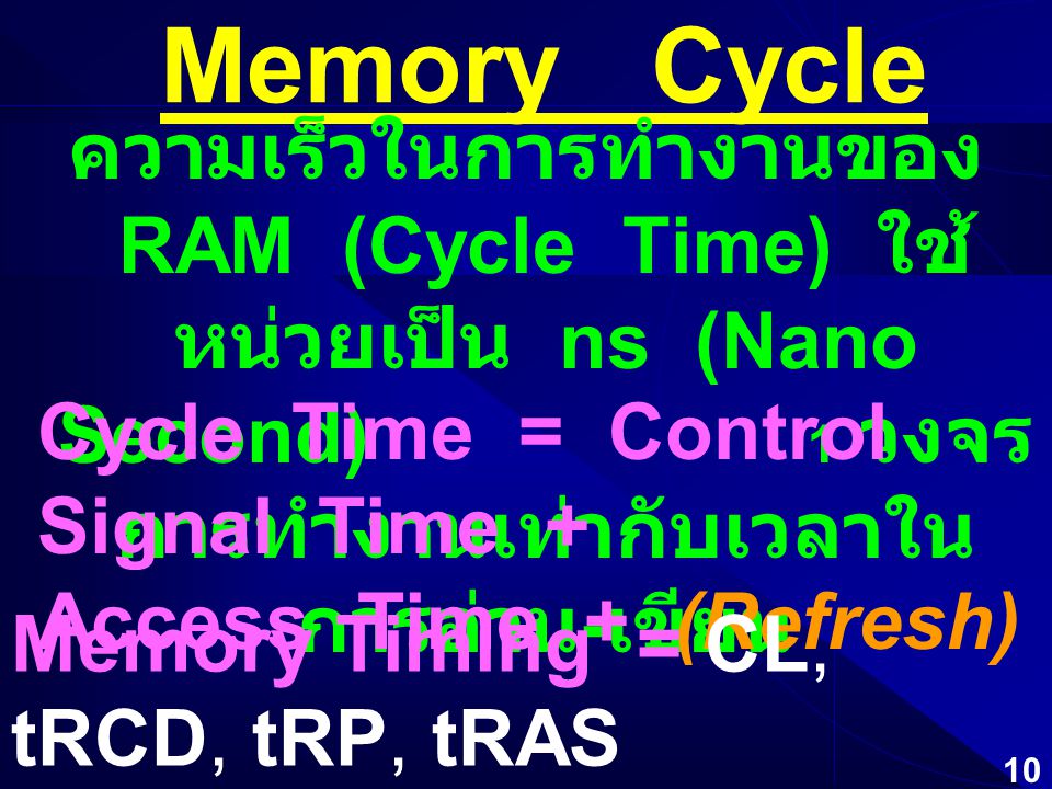
10 Memory Cycle ความเร็วในการทำงานของ RAM (Cycle Time) ใช้ หน่วยเป็น ns (Nano Second) 1 วงจร การทำงานเท่ากับเวลาใน การอ่าน - เขียน Cycle Time = Control Signal Time + Access Time + (Refresh) Memory Timing = CL, tRCD, tRP, tRAS
 ใช้ หน่วยเป็น ns (Nano Second) 1 วงจร การทำงานเท่ากับเวลาใน การอ่าน - เขียน Cycle Time = Control Signal Time + Access Time + (Refresh) Memory Timing = CL, tRCD, tRP, tRAS")
12
Memory Timing CL = CAS latency The time between sending a column address to the memory and the beginning of the data in response. This is the time it takes to read the first bit of memory from a DRAM with the correct row already open. T RCD = Row Address to Column Address Delay The number of clock cycles required between the opening a row of memory and accessing columns within it. The time to read the first bit of memory from a DRAM without an active row is T RCD + CL. 11

13
Memory Timing T RP = Row Precharge Time The number of clock cycles required between the issuing of the precharge command and opening the next row. The time to read the first bit of memory from a DRAM with the wrong row open is T RP + T RCD + CL. T RAS = Row Active Time The number of clock cycles required between a bank active command and issuing the precharge command. This is the time needed to internally refresh the row, and overlaps with T RCD. Typically approximately equal to the sum of the previous three numbers. 12

14
13 Memory Cycle Access Time เป็นเวลาที่ใช้ในการ เข้าถึงข้อมูลหรือเวลาที่ข้อมูลจะถูก ส่งออกไปทาง Data Bus สามารถดู ได้จาก เลขรหัสที่ตัว Memory Chip เช่น HM411000-85 Access time (ns.) ตัวเลขที่แสดงบน Chip 25025 20020 15015 12012 10010 85 808, 80 707, 70 65 606, 60 53
 ตัวเลขที่แสดงบน Chip , , , 60 53")
15
14 Memory Cycle RAM ตอบสนอง CPU ได้ ภายใน 2 Clock Cycles มิฉะนั้นจะ ส่งสัญญาณ /WAIT แจ้ง CPU ให้รอคอย (Wait State)
")
16
Wait State A wait state is a delay experienced by a computer processor when accessing external memory or another device that is slow to respond. As of late 2007, computer microprocessors run at very high speeds, while memory technology does not seem to be able to catch up: typical PC processors like the Intel Core 2 and the AMD Athlon 64 X2 run with a clock of several GHz, while the main memory clock generally ranges from 667 to 1333 MHz. Some second-level CPU caches run slower than the processor core. IntelCore 2AMD Athlon 64 X2GHzMHzCPU caches 15

17
Wait State When the processor needs to access external memory, it starts placing the address of the requested information on the address bus. It then must wait for the answer, that may come back tens if not hundreds of cycles later. Each of the cycles spent waiting is called a wait state.address bus Wait states are a pure waste for a processor's performance. Modern designs try to eliminate or hide them using a variety of techniques: CPU caches, instruction pipelines, instruction prefetch, branch prediction, simultaneous multithreading and others. No single technique is 100% successful, but together they can significantly reduce the problem.CPU caches instruction pipelinesinstruction prefetchbranch prediction simultaneous multithreading 16

18
17 WAIT-STATE Solving Interleave เพื่อลด Refresh Time ปกติใช้เวลา 1 Cycle Time โดย ติดต่อเป็น Block ( ทีละหลาย Address เรียงต่อกัน ) จึงใช้หลักการที่ทำให้ Cycle Time เหลื่อมกัน เพื่อให้ Cycle Time ใหม่มีช่วงที่แคบลง Memory Types Latency Times (Processor Cycle per bit Delivered) Bit 1Bit 2Bit 3Bit 4 L2 SRAM2111 SDRAM5111 BEDO DRAM5111 DRAM5222 FPM DRAM5533 Summary of Memory Data Rate for a 66 MHz. Processor Cycle time with a Memory Page Hit, ranked fastest to slowest

19
18 WAIT-STATE Solving การสลับ Bank ของ Memory โดย Bank หนึ่ง ช่องมี Address เป็นเลขคี่ อีก Bank เป็นเลขคู่ เวลา CPU ติดต่อก็สลับไปมา เพราะฉะนั้นต้องใส่ Memory ให้เต็ม Bank เป็นจำนวนคู่เสมอ การ ใส่เพียง Bank เดียว ทั้งหมด จะทำงานได้ช้า กว่า

20
19 WAIT-STATE Solving Page Mode ต้องใช้ Paged RAM โดย แบ่ง Memory ออกเป็น กลุ่มๆ (Pages) การ ติดต่อ Memory ในกลุ่ม (Page) เดียวกัน จึงไม่ ต้องมี Wait State
 การ ติดต่อ Memory ในกลุ่ม (Page) เดียวกัน จึงไม่ ต้องมี Wait State")
21
20 WAIT-STATE Solving Cache Memory หากรวมอยู่กับ CPU เรียกว่า Internal Cache หากติดบนแผงวงจรหลัก เรียกว่า External Cache มีความเร็วสูงมาก ให้ CPU ติดต่อโดยตรงกับ Cache แทน

22
21 WAIT-STATE Solving วงจร Cache Controller จะจัดการตัด Data Block จาก Memory 2-4 KB. แบบ Random มาใส่ไว้ใน Cache ให้ก่อน CPU จะตรวจสอบก่อนว่ามีข้อมูล ที่ต้องการอยู่ใน Cache หรือไม่ ? ปกติ CPU มักใช้ข้อมูลที่ ต่อเนื่องกัน

23
22 Error Checking Parity and Non-Parity ECC Error Checking and Correcting (ECC) Hamming Code
 Hamming Code")
24
23 Parity and Non- Parity Parity ใช้ Parity Bit เป็นตัวตรวจสอบความ ถูกต้องของข้อมูล เมื่อ พบข้อผิดพลาดจะส่งค่า System Halt Non-Parity ไม่มีการตรวจสอบบิตนี้

25
24 ECC Error Checking and Correcting ทั้งตรวจสอบแล้วยังแก้ไขบิตที่ผิดพลาด ได้ด้วย ( ยกเว้นกรณีที่มีข้อมูลผิดพลาดมากๆ ) ECC-RAM มี Overhead การเก็บข้อมูล มากกว่าแบบ Parity
 ECC-RAM มี Overhead การเก็บข้อมูล มากกว่าแบบ Parity")
26
25 Hamming Code Richard Hamming at Bell Lab. เรียกว่า SEC-DEC : Single- Error-Correcting, Double- Error-Detecting นำมาใช้บนเครื่อง VAX ใช้ 7 Bits ของ SEC-DEC กับทุกๆ 32 Bits ข้อมูล

27
26 Coming Soon 003


 SDRAM นี้ จะต่างจาก DRAM เดิม ตรงที่มันจะทำงานสอดคล้องกับสัญญาณนาฬิกา โดยมีช่วงเวลาในการเข้าถึงข้อมูล ตามที่เราๆมักจะได้เห็นบน.>")

.>")

 AND Extended-Data Output (EDO) DRAM>")


>")
>")


 เลขฐานสอง (Binary Number)>")